With Intel's Developer Forum just days away, an apparently leaked presentation for the event indicates where the chipmaker's processors are headed over the course of the next four years.
It's here, however, that the presentation veers into largely unfamiliar territory. Apart from planning a chip die shrink to 32 nanometers for i7 due later in 2009, known as Westmere, Intel's next big change in architecture is now set to take place in 2010 with a technology known as Sandy Bridge.
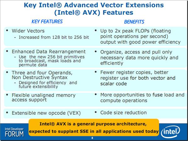
While lightly discussed in the past, Sandy Bridge is now said to focus heavily on vector math — an important component to certain 3D and movie operations and once the strongest selling point of PowerPC-based Macs. The processor design will introduce support for new programming features known as Advanced Vector Extensions, or AVX, which will not only be much more complex with 256 bits of data versus 128 for today's SSE equivalents but will support as many as three or four calculations in one instruction depending on the task at hand.
The overhaul of Intel's chip design will also be built with the capability to handle at least eight cores on a single chip and will have much less Level 2 memory cache than today, at just 512KB per core, in return for 16MB of Level 3 to be distributed among all the cores. This architecture will be shrunk sometime in 2011 when it's known as Ivy Bridge, according to Intel.
For future processors, the Santa Clara, Calif.-based company has less detail but vows a breakthrough at least as significant as Sandy Bridge. Nicknamed Haswell, it will have "revolutionary" power management, an all-new approach to caching, and the option of dedicated vector coprocessors in a package separate from the main processor. It will also be the first Intel chip to support Fused Multiply-Add instructions that, as the name suggests, include math with both additions and multiplications in a lone instruction.
Intel isn't expected to confirm at least some of these details for either Sandy Bridge or Haswell ahead of the Developer Forum, which starts August 19th in San Francisco. With both processor generations not due for at least another two years, though, the presentations made at the event will, for now, be the best look at where mainstream computers will be in the future.